
The performance and memory capabilities of the microcontrollers are increasing, and so is their complexity, especially when the users are responsible for mapping external memory chips such as flash or SPIRAM by configuring a memory management unit.
When I started to use Espressif ESP32’s series SoC’s with the Zephyr RTOS, quickly I realized that these SoC’s are a very different world, compared to my previous MCU experiences, which were mostly ARM-related. ARM Cortex-M’s - in most cases - uses Von-Neumann memory architecture, while the ESP32’s series of microcontrollers uses the Harvard memory architecture, which adds complexity.
The primary source of knowledge about any SoC was always the datasheet or Technical Reference Manual of the part. Indeed it still is, but I found the ESP32’s TRM — although very useful — quite challenging to read. Especially because there is a significant portion of important information buried in the long textual descriptions.
This sparked the motivation to compile a visually rich and informative depiction of crucial information from the current versions of a TRM. This is intended to be used together with the SoC’s datasheets and TRM to help better understand the internals of the ESP32’s series of SoCs internals, which is crucial during the system and driver development - for example when porting to other platforms such as Zephyr RTOS.
ESP32#
The ESP32 is the Xtensa LX6 dual-core microcontroller, and it is the oldest SoC from the ESP32’s series of SoCs.
The SoC has access to external flash memory using the SPI interface. It can also access the external SPIRAM, but only on the data bus.
Zephyr-RTOS support for the ESP32 devkit board can be found here.
ROM
ROM memories hold the primary bootloader code and other library functions available to the end users. The content of the ROM memories is baked during the manufacturing process and cannot be changed. Please refer to the chip versions of the ESP32 microcontroller for more detailed information. In short, please use the lastest chip revision (v3) when working with the ESP32 on Zephyr RTOS.
SRAM
The ESP32 has three internal SRAM modules. The SRAM0 is 192kB, and it can be configured to use the first 64kB as MMU cache for the external memory access. When not used as a cache, the first 64kB can be read and written by either CPU from the instruction bus.
The capacity of Internal SRAM1 is 128 KB. Either CPU can read and write this memory using the data and instruction bus.
The address ranges of the instruction and the data bus are in reverse order (word-wise).
RTC-SRAM
RTC-Fast Memory can be read and written by PRO_CPU only, at a given address range on the data bus or at the instruction bus. Unlike most other memory regions, RTC Fast memory cannot be accessed by the APP_CPU.
RTC-Slow memory is r/w memory that can be accessed by either CPU via the instruction and data bus.
The RTC memories can hold the data during the deep sleep period.
Instruction & data cache
The instruction and data cache address space is a virtual address space where the external memories such as flash or SPIRAM modules can be accessed by the instruction or the data bus.
Internal memories and cache address space#
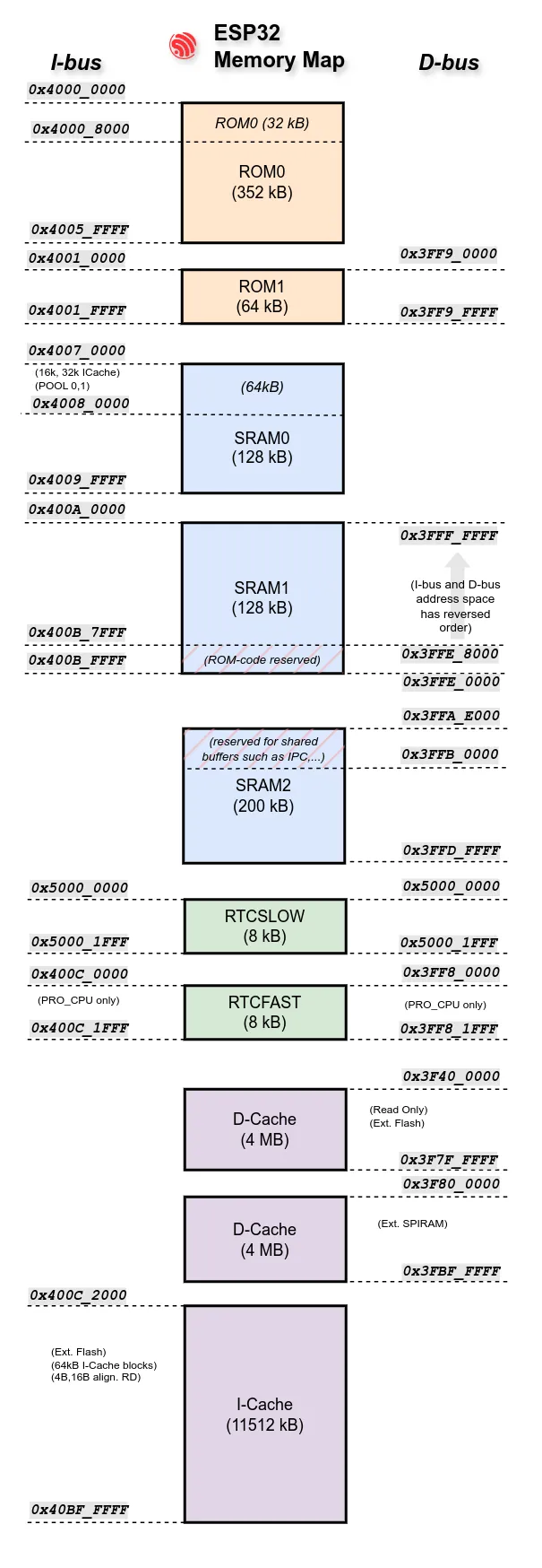
The ESP32 memory map.
Peripheral registers#
The ESP32 has 41 peripherals. Nearly all peripheral modules can be accessed by either CPU at the same address with a single exception of the PID controller which exists for each CPU and can be accessed only by its own CPU.
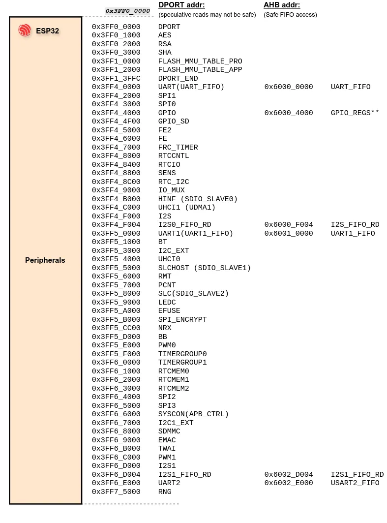
The ESP32 peripherals map.
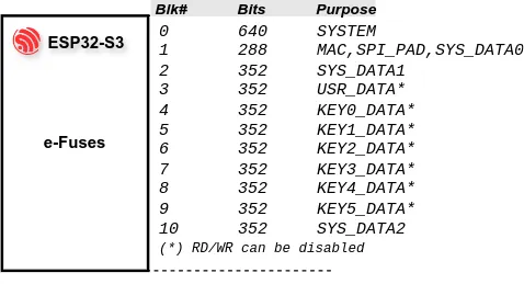
e-Fuse blocks#
The eFuse memory is the OTP (one-time-programmable) memory where hardware and encryption settings are stored. Fundamentally, an eFuse is a single bit of non-volatile memory with the restriction that once an eFuse bit is programmed to 1, it can never be reverted to 0.
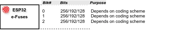
The ESP32 e-fuse map.
For further information and all the details about the ESP32 SoC please refer to the latest ESP32 Technical Reference Manual.
ESP32-S2#
The ESP32-S2 microcontroller is the successor of ESP32 and although very similar it has a single core and slightly different memory composition.
One of the improvements from ESP32 is the ability to access external SPI-ram on data and instruction buses, which means it can run programs and access the data.
Zephyr-RTOS support for the ESP32-S2 devkit board can be found here.
ROM
ROM memories hold the primary bootloader code and other library functions available to the end users. The content of the ROM memories is baked during the manufacturing process and cannot be changed.
SRAM
The ESP32-S2 consists of SRAM0 which can be configured as a hardware cache to access external memories. SRAM1 is r/w memory space addressed by the CPU on the data and instruction bus in the same order.
RTC-SRAM
RTC-Slow memory can be accessed by the CPU via the instruction and data bus. But is also accessible via the peripheral bus 1 and 2.
RTC-Fast is r/w memory that can be accessed by the CPU via the instruction and data bus.
Instruction & data cache
The CPU accesses the external memories using the cache. Up to 7.5MB of address space can be accessed via the I-cache. Up to 4MB of address space can be used to access the I-Cache as read-only via the data bus. Up to 10.5MB of address space can be used to access the external flash or SPIRAM.
Internal memories and cache address space#
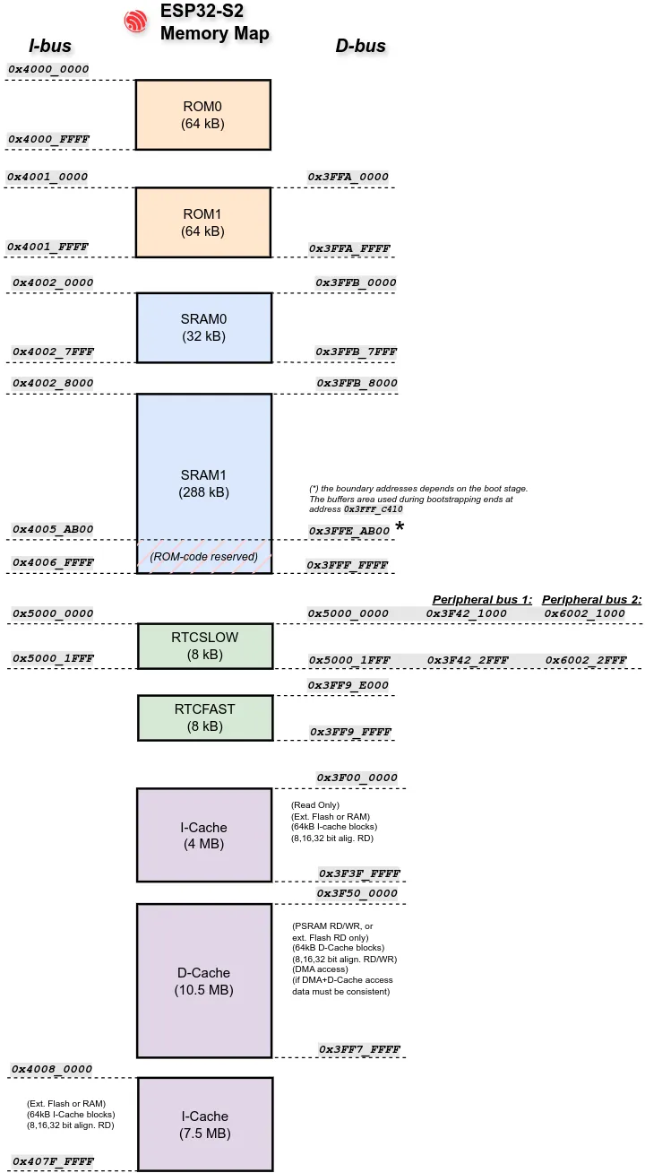
The ESP32 memory map.
Peripheral registers#
The peripherals on ESP32-S2 are accessed using two peripheral busses: PeriBus1 and PeriBus2. Each has its own address space at the data bus.
The PeriBus1 features speculative reads to improve performance. This also means that not every access is valid. Therefore we need to use the volatile statement, or access registers such as FIFOs using the PeriBus2, which is slower but safe.
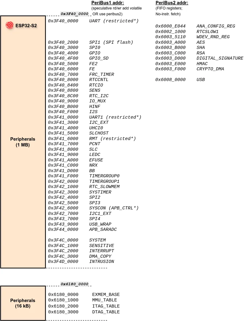
The ESP32-S2 peripherals.
eFuse blocks#
The eFuse memory consists of 4096 bits of OTP (one-time-programmable) memory where hardware and encryption settings are stored. Fundamentally, an eFuse is a single bit of non-volatile memory with the restriction that once an eFuse bit is programmed to 1, it can never be reverted to 0.
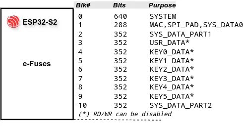
The ESP32-S2 e-fuse block.
For further information and all the details about the ESP32-S2 SoC please refer to the latest ESP32-S2 Technical Reference Manual.
ESP32-S3#
The ESP32-S3 is the latest Xtensa LX7 CPU with a dual-core design. Besides two main cores, it has two ultra-low-power coprocessors based on Risc-V architecture. The SoC has a built-in JTAG debugger accessible via a USB interface. It can access external SPIRAM on data and instruction buses, which means it can run programs and access the data.
Zephyr-RTOS support for the ESP32-S3 devkit board can be found here.
ROM
ROM memories hold the primary bootloader code and other library functions available to the end users. The content of the ROM memories is baked during the manufacturing process and cannot be changed.
SRAM
There are three internal SRAM modules. The SRAM0 can be configured as an I-Cache buffer to access instructions from external memory or be used as static r/w memory via the instruction bus. SRAM1 is the r/w memory which can be accessed via the instruction and data bus. SRAM2 can be configured as D-Cache, or it can be accessed as static r/w memory via the data bus
RTC-SRAM
RTC-Slow is r/w memory that can be accessed via the instruction and data bus. RTC-Fast is the r/w memory that can be accessed via the instruction and data bus on a given address range.
Instruction & data cache
The CPUs can access external memories via the cached MMU address space. Memories can be accessed using I-Cache or D-Dache via instruction or data bus respectively.
Internal memories and cache address space#
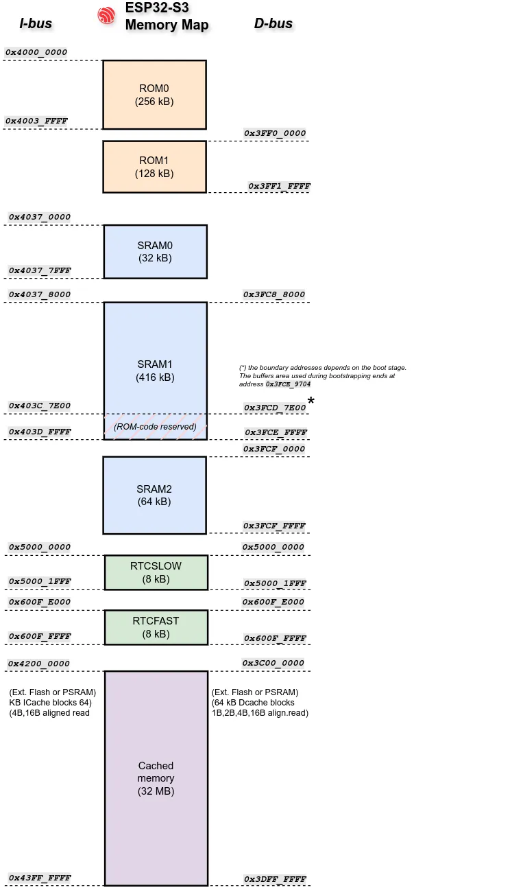
The ESP32 memory map.
Peripheral registers#
The peripherals (modules) can be accessed at their address range using the data and instruction bus. Each peripheral module has its own memory boundaries given by its base address and block size. Blocks size is usually 4kB long. For more details refer to device TRM.
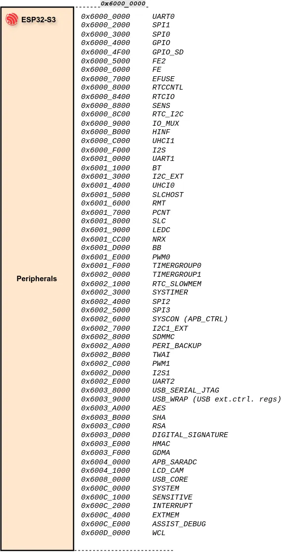
The ESP32-S3 peripherals.
eFuse blocks#
The eFuse memory consists of 4096 bits of OTP (one-time-programmable) memory where hardware and encryption settings are stored. Fundamentally, an eFuse is a single bit of non-volatile memory with the restriction that once an eFuse bit is programmed to 1, it can never be reverted to 0.
The ESP32-S3 e-fuse block.
For further information and all the details about the ESP32-S3 SoC please refer to the latest ESP32-S3 Technical Reference Manual.
ESP32-C3#
The ESP32-C3 is a 32-bit RISC-V microcontroller. The address space of ESP32-C3 is significantly simpler compared to its Xtensa counterparts. It supports JTAG debugging via the on-chip USB interface.
Zephyr-RTOS support for the ESP32-C3 devkit board can be found here.
ROM
ROM memories hold the primary bootloader code and other library functions available to the end users. The content of the ROM memories is baked during the manufacturing process and cannot be changed.
SRAM
The ESP32-C3 has two SRAM modules. SRAM0 can be configured as the instruction cache buffer, or accessed as static r/w memory. The SRAM1 is a general-purpose r/w memory that can be accessed via instruction and data bus.
RTC-SRAM
RTC-Fast memory is r/w memory that can be accessed via CPU instruction and data bus.
Instruction & data cache
The ESP32-C3 supports SPI, dual-SPI, quad-SPI, and QPI interfaces to access the external flash memory. It supports manual encryption and automatic decryption. The external flash can be accessed by the I-Cache or D-Cache on instruction or data bus respectively.
Internal memories and cache address space#
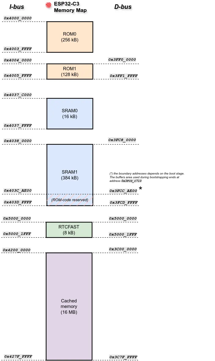
The ESP32-C3 memory map.
Peripheral registers#
The CPU can access the peripherals (modules) using the data or instruction bus on a given address space. Each peripheral has its own memory boundaries given by the base address and block size, which is usually 4kB. For details please refer to the TRM.
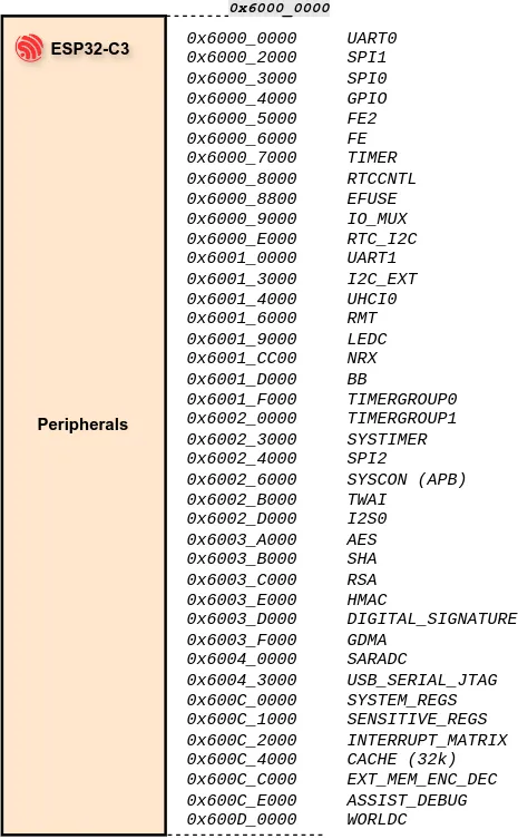
The ESP32-C3 peripherals.
eFuse blocks#
The eFuse memory consists of 4096 bits of OTP (one-time-programmable) memory where hardware and encryption settings are stored. Fundamentally, an eFuse is a single bit of non-volatile memory with the restriction that once an eFuse bit is programmed to 1, it can never be reverted to 0.
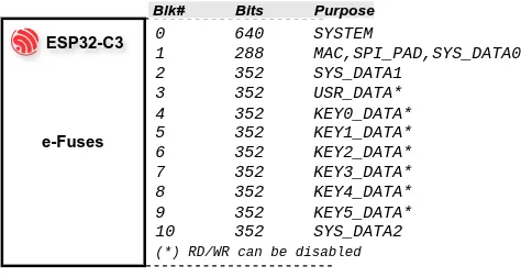
The ESP32-C3 e-fuse block.
For further information and all the details about the ESP32-C3 SoC please refer to the latest ESP32-C3 Technical Reference Manual.
ESP32-C2#
The ESP32-C2 is a low-cost 32-bit RISC-V single-core SoC with Wi-Fi 4 (802.11b/g/n) and Bluetooth LE. The same silicon is also referred to as ESP8684 — Espressif uses that name on modules, dev kits, and in much of the documentation (including the TRM filename), so you will often see ESP32-C2 and ESP8684 used interchangeably.
Zephyr-RTOS support for the ESP8684 devkit board can be found here.
ROM
ROM memories hold the primary bootloader code and other library functions available to the end users. The content of the ROM memories is baked during the manufacturing process and cannot be changed.
SRAM
The ESP32-C2 / ESP8684 integrates on-chip SRAM for code and data, with part of the SRAM budget typically reserved for cache when executing from external flash (XIP). Exact sizes and split between retention-capable regions are defined in the datasheet and TRM for your chip revision.
RTC-SRAM
RTC-Fast memory is r/w memory that can be accessed by the CPU via the instruction and data bus, subject to the address map described in the TRM.
Instruction & data cache
The SoC accesses external flash through SPI (including multi-line modes supported on the part). Cached XIP and the MMU-backed address windows follow the same general model as the other ESP32 RISC-V devices in this article; refer to the TRM for the exact bus layout and region attributes.
Internal memories and cache address space#
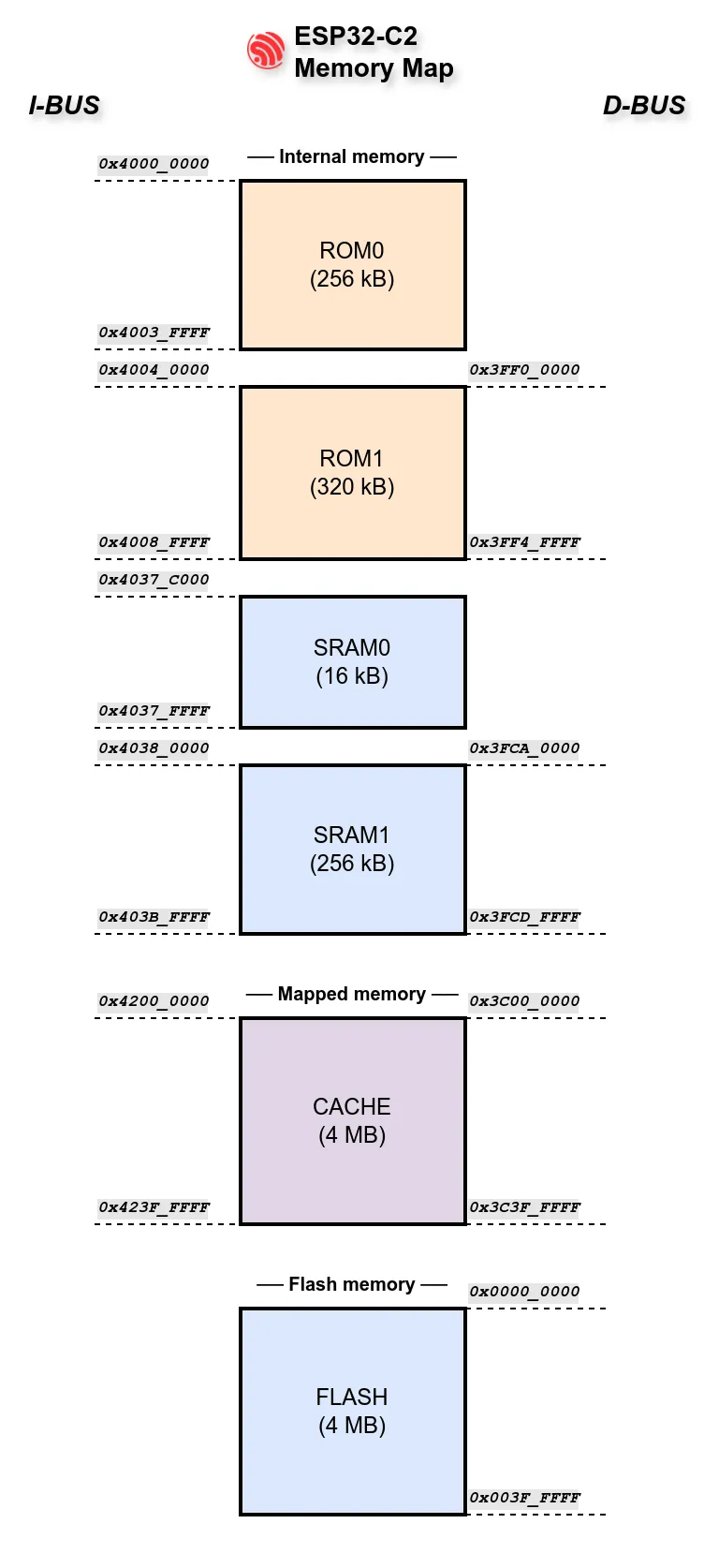
The ESP32-C2 (ESP8684) memory map.
Peripheral registers#
The CPU accesses peripherals through the memory-mapped address space. Each peripheral occupies a region defined by base address and block size in the TRM (typically 4 kB aligned blocks).
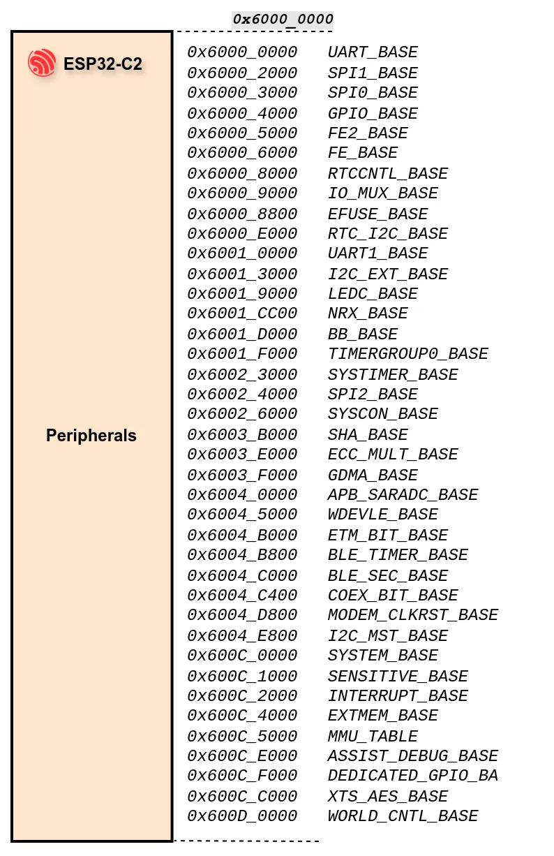
The ESP32-C2 (ESP8684) peripherals.
eFuse blocks#
The eFuse memory is an OTP (one-time-programmable) region used for security configuration, calibration, and other permanent device parameters. Once programmed, bits cannot be reverted.
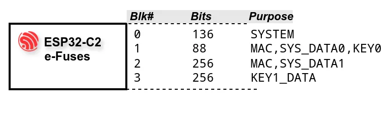
The ESP32-C2 (ESP8684) e-fuse map.
For further information and all the details about the ESP32-C2 / ESP8684 SoC please refer to the latest ESP8684 Technical Reference Manual.
ESP32-C6#
The ESP32-C6 is a 32-bit RISC-V microcontroller with the “IMAC” extensions. The address space of ESP32-C6 is also significantly simpler compared to its Xtensa counterparts. It supports JTAG debugging via the on-chip USB interface.
Zephyr-RTOS support for the ESP32-C6 devkit board can be found here.
ROM
ROM memories hold the primary bootloader code and other library functions available to the end users. The content of the ROM memories is baked during the manufacturing process and cannot be changed.
SRAM
The ESP32-C6 has two SRAM modules.
HP-SRAM is static r/w memory that can be accessed by the HP CPU or LP CPU via the data bus or instruction bus in the same order.
LP-SRAM is static r/w memory that can be accessed by the HP CPU or LP CPU via the data bus or instruction bus. It can be accessed using high-speed more or low-speed more.
Instruction & data cache
ESP32-C6 supports SPI, dual-SPI, quad-SPI, or QPI interface to connect external flash memory. It also supports manual encryption and automatic decryption to protect user data and code.
Internal memories and cache address space#
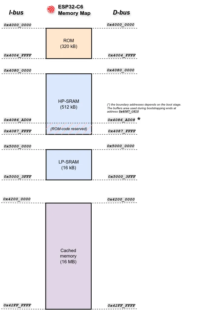
The ESP32-C6 memory map.
Peripheral registers#
The CPU can access the peripherals (modules) using the data or instruction bus on a given address space. Each peripheral has its own memory boundaries given by the base address and block size, which is usually 4kB. For details please refer to the TRM.
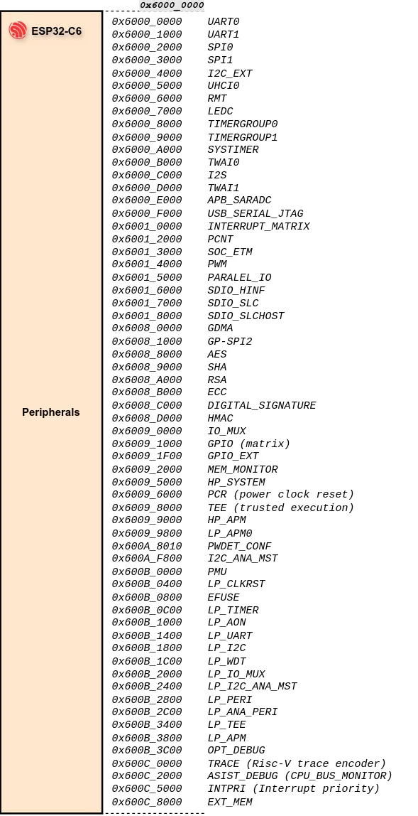
The ESP32-C6 peripherals block.
eFuse blocks#
The eFuse memory consists of 4096 bits of OTP (one-time-programmable) memory where hardware and encryption settings are stored. Fundamentally, an eFuse is a single bit of non-volatile memory with the restriction that once an eFuse bit is programmed to 1, it can never be reverted to 0.
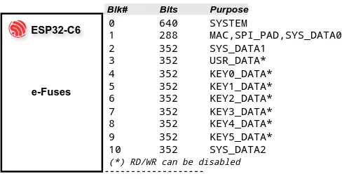
The ESP32-C6 e-fuse block.
For further information and all the details about the ESP32-C6 SoC please refer to the latest ESP32-C6 Technical Reference Manual.
ESP32-C5#
The ESP32-C5 is a 32-bit RISC-V SoC which brings dual-band Wi-Fi 6 (2.4 GHz and 5 GHz) to the ESP32-C family. Besides Wi-Fi 6 (802.11ax, with 802.11a/b/g/n/ac compatibility), it also integrates Bluetooth LE and IEEE 802.15.4 (Thread/Zigbee), with time-division coexistence between the radios. The main CPU (HP core) can run up to 240 MHz and the SoC also includes an LP RISC-V core intended for low-power tasks.
Zephyr-RTOS support for the ESP32-C5 devkit board can be found here.
ROM
ROM memories hold the primary bootloader code and other library functions available to the end users. The content of the ROM memories is baked during the manufacturing process and cannot be changed.
SRAM
ESP32-C5 contains internal SRAM used for both code and data (384 KB HP SRAM plus 16 KB LP SRAM), and 320 KB of ROM. External flash is accessed via SPI (XIP), and designs can also add external PSRAM which becomes visible through cache/MMU-backed windows.
Instruction & data cache
Just like the other ESP32 families, the ESP32-C5 uses an MMU-backed cached address space to execute from external flash (XIP) and to access external RAM (PSRAM) if present. From a system/driver-development point of view, the key concept remains the same: the CPU sees a virtual address space, while the external flash/PSRAM is accessed through cache-backed windows.
Internal memories and cache address space#
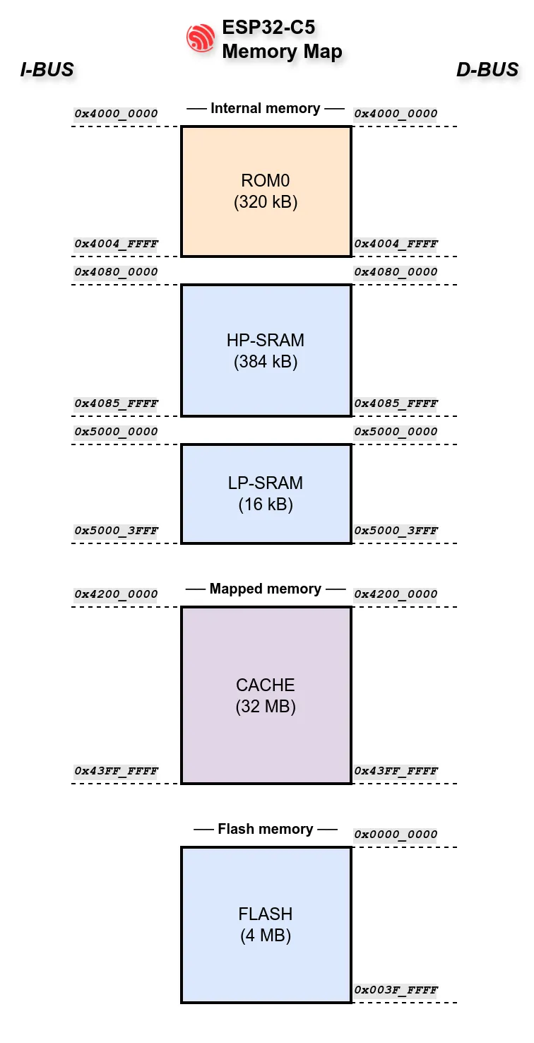
The ESP32-C5 memory map.
Peripheral registers#
Peripherals are accessed using the memory-mapped peripheral address space. As in the other ESP32 SoCs, peripherals typically occupy fixed-size regions (often 4 kB blocks) defined by a base address plus an offset map in the TRM.
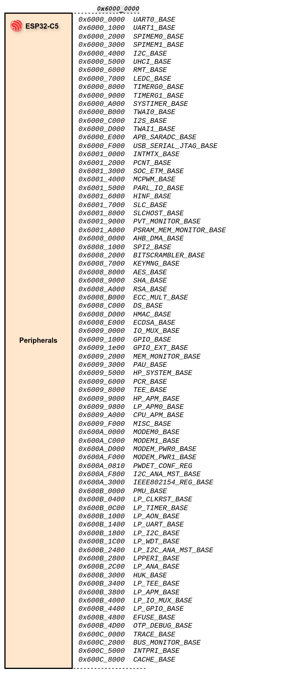
The ESP32-C5 peripherals block.
eFuse blocks#
The eFuse memory is an OTP (one-time-programmable) region used to store device configuration, calibration data, and security settings. Once programmed, bits cannot be reverted.
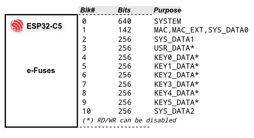
The ESP32-C5 e-fuse map.
For further information and all the details about the ESP32-C5 SoC please refer to the latest ESP32-C5 Technical Reference Manual.
ESP32-H2#
The ESP32-H2 is a low-power 32-bit RISC-V SoC focused on IEEE 802.15.4 and Bluetooth LE connectivity. It supports Thread and Zigbee over 802.15.4, plus Bluetooth LE (including mesh and long-range coded PHY options), which makes it a good fit for Thread/Zigbee end-devices and for Matter-over-Thread commissioning via Bluetooth LE. Unlike most other ESP32 SoCs, it does not include Wi-Fi. The CPU can run up to 96 MHz.
Zephyr-RTOS support for the ESP32-H2 devkit board can be found here.
ROM
ROM memories hold the primary bootloader code and other library functions available to the end users. The content of the ROM memories is baked during the manufacturing process and cannot be changed.
SRAM
ESP32-H2 contains 320 KB of SRAM (plus cache), 128 KB ROM, and small low-power memory regions intended for low-power operation modes. Common variants integrate 2 MB or 4 MB of in-package flash, which simplifies the external memory setup compared to designs that route flash pins out to the board.
Instruction & data cache
Compared to the Wi-Fi capable families, ESP32-H2 is simpler: typical designs use the in-package flash variants, but the same general concept applies — code is executed from flash using cached/XIP regions, while SRAM is used for runtime data and time-critical code/data placement when needed.
Internal memories and cache address space#
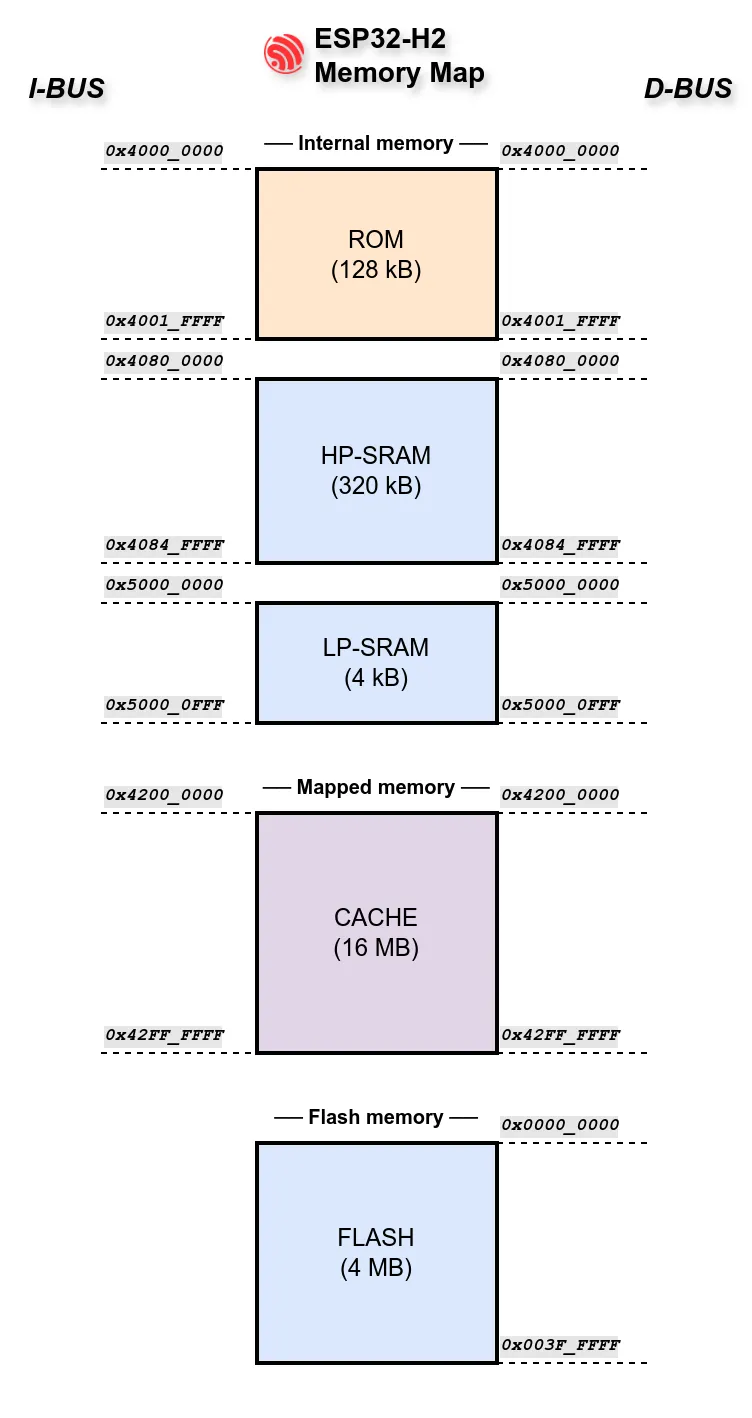
The ESP32-H2 memory map.
Peripheral registers#
Peripherals are accessed via memory-mapped registers. Each peripheral module has its own base address and register layout described in the TRM.
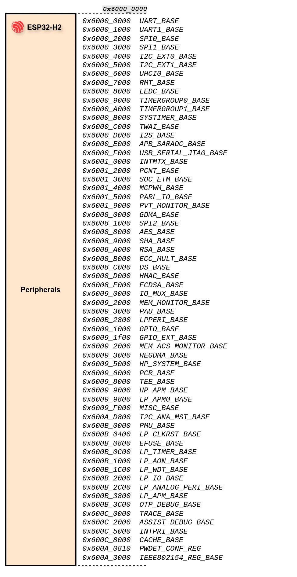
The ESP32-H2 peripherals block.
eFuse blocks#
The eFuse memory is an OTP region used to store security configuration (e.g. secure boot / flash encryption related settings), calibration values, and other permanent device parameters.
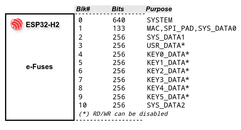
The ESP32-H2 e-fuse map.
For further information and all the details about the ESP32-H2 SoC please refer to the latest ESP32-H2 Technical Reference Manual.
ESP32-P4#
The ESP32-P4 is a high-performance RISC-V SoC designed for compute-heavy applications (HMI, audio/voice, image processing), with a dual-core HP system (up to 400 MHz) and an LP core (up to 40 MHz) for low-power tasks. It also integrates high-speed peripherals such as USB 2.0 OTG (including high-speed), Ethernet MAC, SDIO Host, and MIPI CSI/DSI. Unlike the chips above, ESP32-P4 does not include integrated Wi-Fi/Bluetooth/802.15.4 — it is typically paired with a wireless companion chip (for example an ESP32-C or ESP32-S series device) when connectivity is required.
At the time of writing, ESP32-P4 is not yet available as a Zephyr board target in upstream documentation. If you are tracking Zephyr enablement, Espressif maintains a public status page here.
ROM
ROM memories hold the primary bootloader code and other library functions available to the end users. The content of the ROM memories is baked during the manufacturing process and cannot be changed.
SRAM
ESP32-P4 has a relatively large on-chip SRAM pool in the HP system (768 KB), plus smaller low-power SRAM for the LP system (32 KB), and a small TCM RAM region (8 KB). This is important when bringing up drivers and multimedia workloads where internal bandwidth and deterministic access matter.
Instruction & data cache
ESP32-P4 can use external memory (flash and/or PSRAM, depending on the variant/board design) and maps it into the CPU address space through cache-backed regions. For performance-sensitive code and data, you typically want to understand which regions are cached, which are internal SRAM, and which are intended for DMA-capable buffers.
Internal memories and cache address space#

The ESP32-P4 memory map.
Peripheral registers#
ESP32-P4 includes high-speed peripherals (e.g., USB 2.0 OTG and Ethernet MAC) in addition to the common ESP peripherals. As always, low-level driver work starts with a good understanding of the peripheral base addresses, register blocks, and the interrupt routing described in the TRM.

The ESP32-P4 peripherals block.
eFuse blocks#
The eFuse memory is an OTP region used for security configuration, device identity, and calibration. For security-related work (secure boot, flash encryption, key provisioning), the eFuse map is often the first place to start.

The ESP32-P4 e-fuse map.
For further information and all the details about the ESP32-P4 SoC please refer to the latest ESP32-P4 Technical Reference Manual.
Downloads#
Printable versions of the images in PDF format can be downloaded here:
Conclusion#
Sometimes, when we need to understand something in-depth, we need to do a deep dive into very technical documents and extract the information in a way that we can use. Technical documents can be challenging to understand, especially when you are not familiar with a particular architecture or if you are not from that specific area. I hope that with this article, you will be able to easily understand the memory map of the ESP32 series of SoCs and use it as a guide when diving deep into the TRMs and datasheets.